Overview
For BU Rocket Team I needed a quick way to test E-Matches and get two readings off of then, namely current draw and to monitor voltage sag from a 3.7V Lithium Ion battery which will eventually be powering the board that is controlling the motor.
At first I tried to test using an IRF820 I found. The main reason was that I could quickly breadboard a test rig, get my data and call it a day. However, the devil is in the details, because at 3.7V this transistor simply can't draw more than 50mA or so. However, for the actual controller board, called Firestarter, I was going to use SI2308BDS N-Channel FETs, which have a much nicer V_ds vs I_ds curve for our application. The SI2308s only come in a SOT-23 package. There are methods to get around this, but I decided to take the opportunity to try PCB Etching.
Table of Contents
Design Phase^
Schematic^
COMING SOON
BOM^
COMING SOON
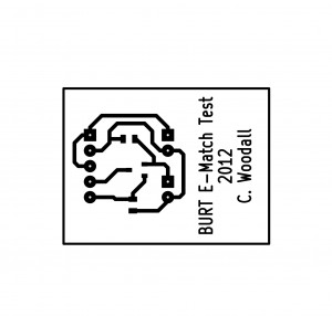
PCB^
This is the bottom of my PCB board, mirrored for printing.
Sources^
Everything can be found on the BURT github here
Etching the PCBs^
Making the Transfers^
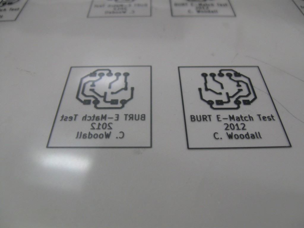
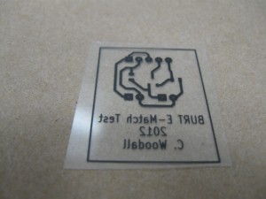
To make the transfers I simply plotted postscript files from KiCAD. It will mirror the back layer automatically. I then converted the postscripts to PDFs and sent them to Kinkos to print transparency's.
I had mixed results with Kinko's transparency's when it came to getting the toner on the right side. Sometimes an employee will try to help and mirror your printout. It took me a while to get them to print it out right, but they were very helpful and sympathetic. Also, you can order them online for 75 cents per page, which is rather affordable.
Cleaning the Copper^
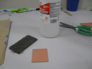
The most important part of etching a PCB is cleaning the surface you are etching on to. I used Isopropyl Alcohol, steal wool and water and dish detergent. Once clean do not touch the copper, the cleaner the surface the better the transfer.
Making the Transfer^
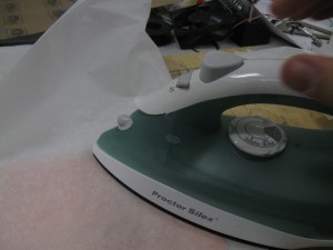
To make the actual transfer I used a clothes iron set to cotton. I then put the transparency of my layout tonerside down onto the board. In retrospect you should also clean your transparency before you try to make the transfer. I covered the transparency with parchment paper and let the iron sit there for 2 minutes, the moved it around gently for about 5 minutes.
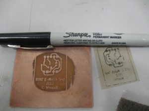
The first time I made the transfer it came out perfect, but on my second attempt I heated it up too much and I had weird results. and needed to touchup using sharpie marker.
Etching^
I used a method that used Ferric Chloride and a sponge. I am not going to explain how exactly to use this method, but instead give some notes on the process. TechShopJim from TechShop wrote a really good Instructables on this method.
Notes:
- Use 1/2oz copper clad if you can find it. You can etch it faster, which is preferable for this method because you can control where the Ferric gets applied.
- Use two cups of water. One is to stop the reaction between the Ferric and copper. However, I noticed that even after one cup of water I got some more etching, so I dumped it into a second cup of water and this stopped the reaction completely.
- Thoroughly rinse the boards afterwards. The Ferric is likely still somewhat present.
- Apply the Ferric from the edges inward. Give more focus to the edges than the center, despite the temptation to really scrub the center. TechShopJim makes this warning and it is a good one.
- Use Acetone to remove the toner faster if you cant. However, Isopropyl will work and I like to scrub the boards down afterwards with some steel wool anyway.
Drilling^
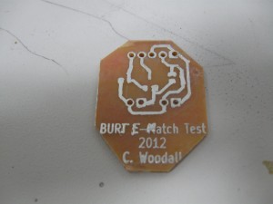
I won't cover the drilling process in depth, except to say two things: Utilize a drill press if you have one; and know what drill bit you are looking for and verify you can access it and use it before hand. I utilized a drill press with a .041 inch drill bit. Since I only etched one side of the board (technically the bottom side), I used a larger drill bit and my hand to burr the top side and create a larger no copper zone around each pin. This is very effective.
Tinning^
Tinning a finished board is important to prevent oxidation. I used leaded solder (60/40), lots of flux, and copper braid.
First, coat your board in rosin. Go crazy if you have flux off, otherwise you might want to be conservative because its hard to remove flux. Now take your soldering iron and get a nice glob of solder built up onto the edge of it. Take this glob and wipe it over your copper traces. You might get some shorting, but the flux should prevent this. You will notice that everything is raised up an uncomfortable amount.
The key is to use copper braid to remove excess solder. So heat of some braid and wipe your board down a few times being careful not to pull up traces or cause any major shorts. Since your holes aren't plated getting solder in holes shouldn't be a problem. Keep applying braid to large globs until you have a nicely tinned board.
Conclusion^
Being able to do your own PCB etching is pretty freeing for prototyping on the fly under tight time constraints; however, it is a nuanced and time consuming process (both times it took me about an hour to two hours). In general, it is also rather costly and with options like OSH Park and Seeed Studio if you have time you should just order your PCBs.
The test results will be coming soon!
